Introduction:
(written 5-20-2007)
Fall 2001 - the beginning of my Junior Year in High
School - the class assignment in Electronics II was to assemble a 0-9VDC
power supply kit, but my teacher, Mr. Doug Ripka, aware that I had already
learned most of the Electronics II curriculum from the books I'd read during my
summer vacation, allowed me to design & construct my own more advanced
power supply. I had spent all of summer 2001 studying books like Basic
Electronics Theory, Power Supplies, Switching Regulators, Inverters, and
Converters, & Building Power Supplies, and having
already built a few gadgets over the summer, I knew very well the thrill of
invention and was eager to revive the feeling with my design, assembly, &
operation of the following project.
±30V DC
1.5A Adjustable Power Supply
Devin
R. Ott
Design - November 2001
Final Assembly - December 2001
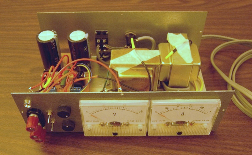
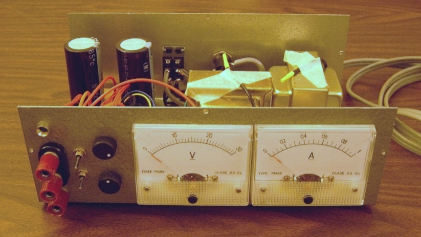
Description:
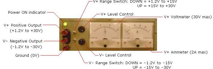
Two independently adjustable DC
power supplies; one positive (V+), one negative (V-). High/Low output ranges.
• 1.5A maximum output current.
• 0.01%/V typical line regulation. • Integrated short circuit protection
& thermal shutdown.
Schematic:
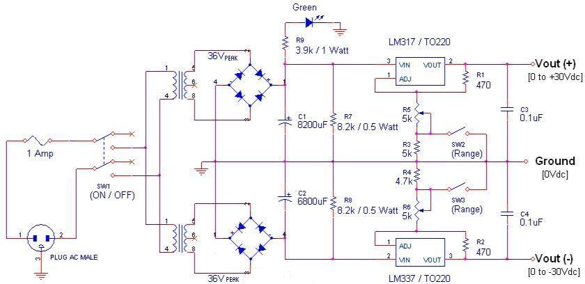
Circuit Operation:
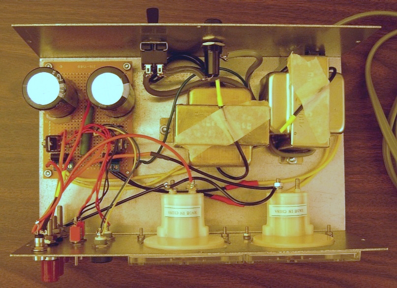
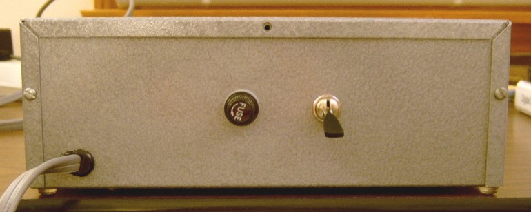
120VAC enters back panel via 16AWG
power cord. Earth GROUND is hardwired to aluminum chassis (10" x
3.5" x 5.8"). Fused AC power is switched by SW1, mounted on
back panel near fuse holder.
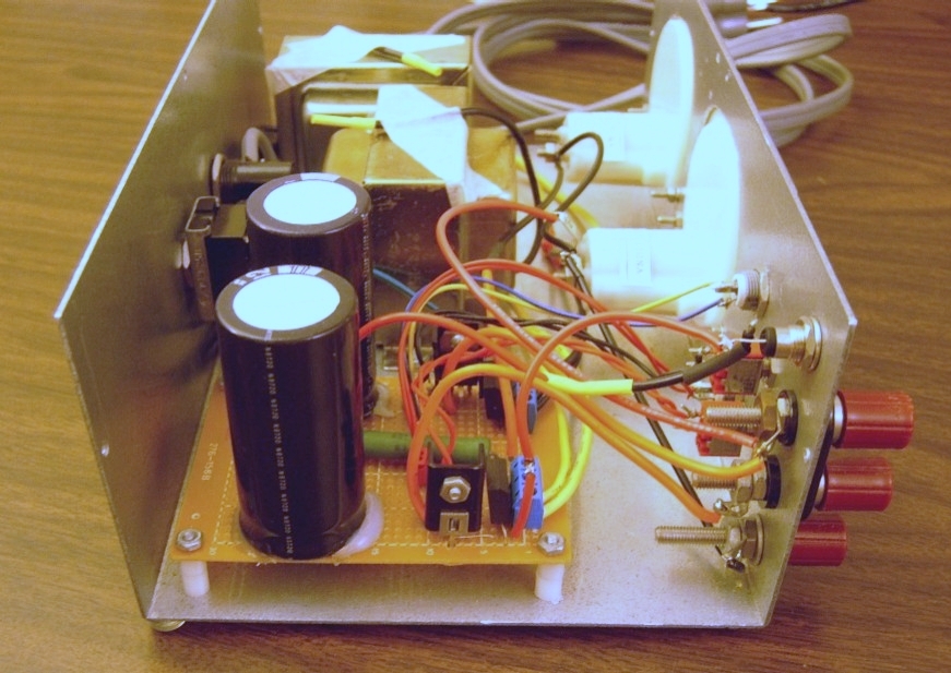
When powered-ON, 120VAC feeds the primary windings of two center-tapped 2A
power transformers (RadioShack #273-1512B), each yielding an isolated 36V-PEAK (25.2V-RMS)
on the secondary winding. The 36V-PEAK is rectified by a 1.5A bridge
rectifier (Fairchild #KBP005M).
Each rectifier outputs a 60Hz pulsing 35V-PEAK DC potential: one is positioned
above GROUND and filtered by C1; the other is positioned below GROUND (V-) and
filtered by C2.
Bleeder resistors {R7, R8} are placed across filter capacitors {C1, C2}
allowing them to discharge when device is powered-OFF. Capacitive time
constant approximation T=RC ≈ 1 minute.
Green LED indicator is biased by the voltage across C1, forcing 9mA forward
current when the device is powered-ON.
The 35VDC on each capacitor is further filtered and regulated by a LM317/LM337
adjustable (positive/negative) voltage regulator, rated for 1.5A and mounted to
a heat sink. Each regulator outputs a low-ripple DC voltage determined by
two external resistances:
• resistance between V-OUT terminal and ADJUST terminal,
{R1, R2}.
• resistance between ADJUST terminal and GROUND reference,
{RADJ}.
The regulated voltages are determined by the following relationship:
LM317:
VOUT = (1.25V)[1+(RADJ÷R1)] + (IADJ)(RADJ)
LM337:
-VOUT = (-1.25V)[1+(RADJ÷R2)] + (-IADJ)(RADJ)
*If the maximum value of RADJ is low (a few kΩ), the voltage
contributed by the (IADJRADJ) term is negligible so it
can be omitted from the VOUT expression.
*Always breadboard & test a new circuit design before you begin its final
layout & assembly. A circuit may work theoretically on paper or in
PSpice, but that doesn't guarantee it'll work in the real world or in your
particular environment of operation. In my own designs, I usually draw
out circuits on paper and then breadboard the design in stages, one after
another, testing each stage as I go, until the entire circuit is on the
board. And for troubleshooting purposes, I always try to leave the breadboard
intact while I layout & assemble the final prototype.
{R1, R2} are fixed at low values.
*see my Voltage
Regulator Experiment for more information.
RADJ is adjusted via potentiometer {R5 or R6} to
vary the regulator's output voltage across two Δ15V ranges.
Switches {SW2, SW3} select one of two VOUT ranges by either
inserting or bypassing a fixed resistor {R3, R4} in series with each
potentiometer.
Positive Supply Voltage: LM317
• SW2 closed ( low range: +1.2 to +15V )
---> RADJ = R5
• SW2 open ( high range: +15 to +30V )
---> RADJ = R5 +
5kΩ
Negative Supply Voltage: LM337
• SW3 closed ( low range: -1.2 to -15V )
---> RADJ = R6
• SW3 open ( high range: -15 to -30V )
---> RADJ = R6 + 4.7kΩ
Output capacitors {C3, C4} prevent the load from exhibiting certain low level
capacitance (a few nF) that can cause oscillations on the regulator's
output. And like all bypass caps, they reduce power line impedance and
effective pick-up loop area.
Final
Assembly:
Improvements:
Improve regulator performance &
stability: My high school electronics teacher, Doug Ripka, always used to
say that "a voltage regulator is like a high-gain amplifier."
• 0.1uF bypass capacitor on
regulator's V-IN terminal - decouples high frequency input noise.
• 10uF bypass capacitor on
regulators ADJUST terminal - improves low frequency ripple rejection,
*consider diode protection to
prevent capacitor from discharging through low-current paths inside the
regulator, causing damage.
*See my 9VDC Supply for SONY Stereo.
•
Electrolytic or tantalum output capacitor (at least 1uF) - prevents low-values
of load capacitance (a few nF) that can cause oscillations on the regulator's
output.
*diode should be used to prevent
output capacitance from discharging through the regulator.
Back to my
EE Page
Back to Home
© 2007, Devin R. Ott