Introduction: (written
9-3-06)
This
experiment was a stepping-stone on my path to designing an engine-controlled
neon light power supply circuit.
The output potential of a typical voltage regulator depends on the voltage of
it's ground reference. This ground reference sinks a mere ~5mA, and can
therefore be supplied by the output of a standard op-amp. Thus, a
high-power supply voltage can be controlled by a low-power reference voltage; a
function very useful in a variety of applications.
This capability/technique is so deep in my knowledge of EE solutions that it's
hard to believe I ever questioned it - it's so obvious.
So if you design circuits and you've never considered this technique - check it
out!
Controlling a Voltage Regulator using an Op-Amp
Devin
R Ott
Design
- completed in August 2004
A voltage regulator
performs the function of stabilizing its output voltage to a certain potential
difference relative to its ground pin. The regulator’s supply voltage
provides it with output power, while the voltage at the ground pin (VGND)
acts as a reference for the device to regulate its output voltage above. Under
normal circumstances, VGND would be tied to the ground potential of
the circuit, so if it was a 5 volt regulator, the output voltage would be 5
volts above ground. However, since the reference at VGND is
required to sink only a few milliamps from the ground pin, this potential can
theoretically be supplied by the output of an operational amplifier.
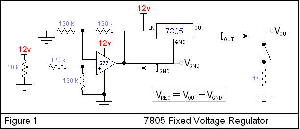
The circuit in figure 1
can test this concept using a 7805 positive 5 volt regulator. The
potential at VGND is supplied by the output of a difference
amplifier circuit built around the OPA277. It functions like a
non-inverting unity-gain DC amplifier that regulates its output (VGND) according to the voltage at the wiper of
the 10k potentiometer. As VGND increases, VOUT should
increase at an equal rate.
The table below compares the
data of the unloaded circuit to the data obtained when VOUT was loaded
with a 47Ω resistor. As VGND was adjusted from about 2
volts to 5 volts, the regulated potential difference (VREG) stayed
reasonably consistent at about 4.93 volts, and was not affected by
loading. However, the data suggests that when the regulator was loaded
with 47Ω, the op-amp’s output voltage (VGND) was slightly
weakened by an average of 52mV, causing VOUT to decrease along with
it.
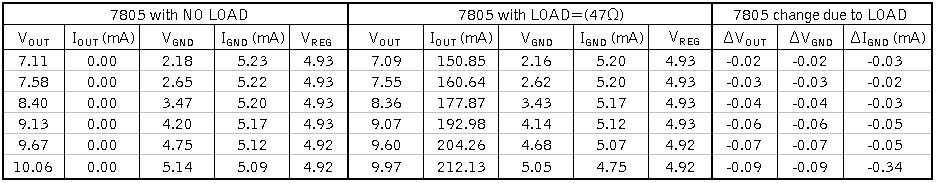
The drop in VGND
was also accompanied by a slight decrease in IGND by an average of about
40nA, when the regulator was loaded. The 7805 regulator has a minimum 2 volt
drop from the input to output. As expected, when VOUT got to within
2 volts of the supply voltage, the loading of the regulator began to have an
increasing affect on IGND, causing it to decrease dramatically. Overall,
the 5mA of current flowing out of the regulator’s ground pin had little effect
on the op-amp’s output voltage (VGND). For most applications,
the slight 50mV fluctuations in VOUT due to loading would be
insignificant.
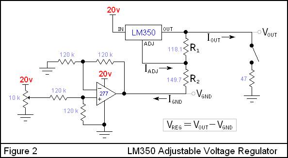
The circuit in Figure 1 showed
that the op-amp’s output voltage remained relatively stable when used as the
ground reference of a fixed voltage regulator. Figure 2 illustrates a similar
design, using the LM350 adjustable voltage regulator in place of the 7805 fixed
regulator. The VREG of the LM350 is determined by the two resistors
R1 and R2, and the current flowing out of the devices
adjustment pin (IADG). This circuit is supplied with 20 volts
to provide a larger range of adjustment.
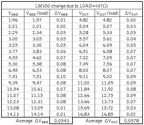
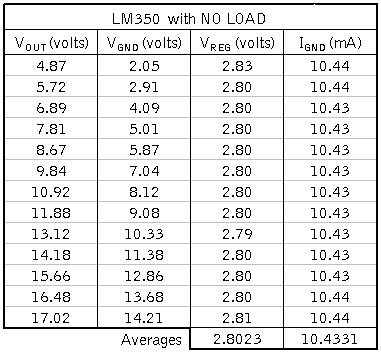
The regulated potential difference
(VREG) of the LM350 regulator in Figure 1 has been programmed to
2.80 volts. As seen in the data from the unloaded LM350, the current flowing
into the op-amp’s output is 10mA, twice the current of the 7805 circuit. Despite
the increased current flowing into the op-amp’s output, the voltage VGND
was not weakened by the loading of the regulator. In fact, VGND
actually increased in response to the regulators load, by about 55mV on
average, causing VOUT to do the same.
As previously stated, the regulated
potential difference VREG is determined not only by the two resistors
R1 and R2, but also by the current flowing out of the
adjustment pin (IADG). Ohm’s law can be used to derive an equation
for IADG in terms of VREG, IGND, R1
and R2. However, ohm’s law cannot predict how the VIN-VOUT
voltage difference will affect the adjustment current. With R1=120Ω
as recommended by the datasheet, the change in IADJ due to the VIN-VOUT
potential is negligible, so the output voltage is not affected by the
regulators input supply voltage.
For other resistor combinations,
such as R1=2kΩ and R2=820Ω, IADJ is
dramatically affected by the regulators VIN-VOUT potential
difference. In this case, as VGND changes, so does the VIN-VOUT
potential, causing IADJ and thus VREG to change as
well. At the lower end of the range, VREG was 3 volts, and by
the upper end of the range, VREG had dropped to 2 volts.
In
conclusion, a voltage regulator can be safely adjusted via the ground reference
VGND, while maintaining reasonably high VOUT stability
relative to the current load (IOUT).
Back to my EE Page
Back to Home
© 2006,
Devin R. Ott